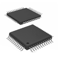

Bilder sind nur zur Referenz
SN54HC00J
54HC00 QUADRUPLE 2-INPUT POSITIV
- Hersteller
- Fr. Teil #SN54HC00J
- Paket
- Datenblatt SN54HC00J DataSheet
- Auf Lager2067
100% Original und Neu
24 Stunden bereit zum Versand
365 Tage Garantie
RFQ & Erhalten Sie mehr Rabatte
Spezifikationen
| Package | Bulk |
| ProductStatus | Active |
Übersicht
Description
Designed for operation from a wide voltage range (typically 3V to 15V), the SN54HC00J is characterized by low power consumption and high noise immunity. It is suitable for both TTL and CMOS logic environments. The package type “J” indicates a ceramic dual in-line package (DIP), suitable for through-hole mounting.
Applications include digital signal processing, arithmetic operations, and state machine designs. Its reliability and performance in military and industrial environments make it a popular choice for engineers and designers.
Features
1. High-Speed Operation: It offers fast switching times, making it suitable for high-frequency applications.
2. Wide Supply Voltage Range: Operates typically between 2V to 6V, compatible with various logic families.
3. Low Power Consumption: The HC series is designed for low power usage, enhancing battery life in portable devices.
4. TTL Compatibility: Compatible with TTL outputs, making it easy to interface with other logic families.
5. Robust Performance: The device is designed to withstand a wide range of temperature and environmental conditions.
6. Pin Configuration: Comes in a 14-pin Dual In-Line Package (DIP), making it easy to integrate into circuit designs.
7. High Noise Immunity: Offers good noise margins, ensuring reliable operation in noisy environments.
Overall, the SN54HC00J is ideal for digital logic circuits, providing versatility and reliability in various applications.
Package
Pinout
1. Pins 1, 2: Input A of the first NAND gate.
2. Pin 3: Input B of the first NAND gate.
3. Pin 4: Output of the first NAND gate.
4. Pin 5, 6: Input A of the second NAND gate.
5. Pin 7: Input B of the second NAND gate.
6. Pin 8: Output of the second NAND gate.
7. Pin 9, 10: Input A of the third NAND gate.
8. Pin 11: Input B of the third NAND gate.
9. Pin 12: Output of the third NAND gate.
10. Pin 13, 14: Input A of the fourth NAND gate and Input B of the fourth NAND gate, respectively.
11. Pin 14: Output of the fourth NAND gate.
The IC operates in a wide voltage range and is suitable for various digital logic applications.
Manufacturer
Application
Equivalent
Versand
VersandmethodenWir
bieten Sie globale Versanddienstleistungen durch DHL, FedEx, TNT, UPS oder einen anderen Spediteur Ihrer Wahl.
Versandgebührenreferenz (DHL/FedEx):
DHL: Versandkosten reichen von $25-$45 (0.5kg), mit einer geschätzten Lieferzeit von 2-5 Werktagen.
von FedEx: Versandkosten reichen von $25-$40 (0.5kg), mit einer geschätzten Lieferzeit von 3-7 Werktagen.
UPS: Versandkosten reichen von $25-$45 (0.5kg), mit einer geschätzten Lieferzeit von 3-7 Werktagen.
TNT: Versandkosten reichen von $25-$65 (0.5kg), mit einer geschätzten Lieferzeit von 3-7 Werktagen.
EMS: Versandkosten reichen von $30-$50 (0.5kg), mit einer geschätzten Lieferzeit von 7-15 Werktagen.
Registrierte Luftpost: Versandkosten sind $ 2- $ 4 (0,1 kg), mit einer geschätzten Lieferzeit von 5-20 Werktagen.
Zahlungen
Payment Methods
Die Zahlungsfrist ist 100% Prepaid.
Derzeit akzeptieren wir nur die folgenden Zahlungsmethoden:
1. PayPal
2. Kredit- / Debitkarte
3. Überweisung
Ähnliche
-
![MX29F400CBTI-70G]() MX29F400CBTI-70G
Macronix
-
![MX66U1G45GXDI00]() MX66U1G45GXDI00
Macronix
-
![MX25V4035FZUI]() MX25V4035FZUI
Macronix
-
![MX25V2033FM1I]() MX25V2033FM1I
Macronix
-
![MX25L25673GMI-10G]() MX25L25673GMI-10G
Macronix
-
![MX29GL512FHXFI-11G]() MX29GL512FHXFI-11..
Macronix
-
![MX25U51279GXDR00]() MX25U51279GXDR00
Macronix
-
![MX25L6433FM2I-08G]() MX25L6433FM2I-08G
Macronix
-
![MX25L12833FZNI-10G]() MX25L12833FZNI-10..
Macronix
-
![MX25U25645GXDI00]() MX25U25645GXDI00
Macronix
-
![MX29LV160DTTI-70G]() MX29LV160DTTI-70G
Macronix
-
![MX25L25645GXDI-08G]() MX25L25645GXDI-08..
Macronix