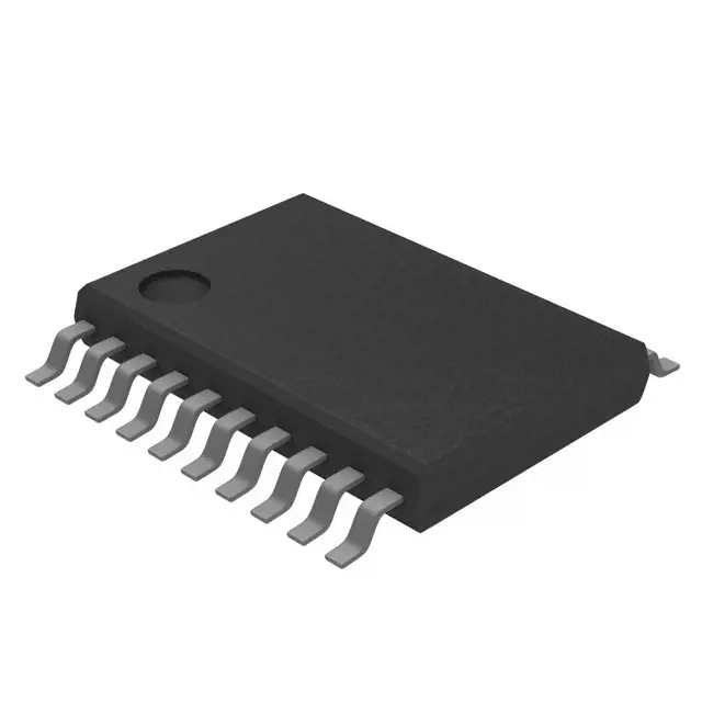
Bilder sind nur zur Referenz
SN74LV373ADW
IC OCT D TRANSP LATCH 20-SOIC
- Hersteller
- Fr. Teil #SN74LV373ADW
- Paket 20-SOIC (0.295, 7.50mm Width)
- Datenblatt
- Auf Lager7549
100% Original und Neu
24 Stunden bereit zum Versand
365 Tage Garantie
RFQ & Erhalten Sie mehr Rabatte
Spezifikationen
| Package | Tube |
| Series | 74LV |
| ProductStatus | Active |
| LogicType | D-Type Transparent Latch |
| Circuit | 8:8 |
| OutputType | Tri-State |
| Voltage-Supply | 2V ~ 5.5V |
| IndependentCircuits | 1 |
| DelayTime-Propagation | 1ns |
| Current-OutputHighLow | 16mA, 16mA |
| OperatingTemperature | -40°C ~ 85°C |
| MountingType | Surface Mount |
| Package/Case | 20-SOIC (0.295, 7.50mm Width) |
Übersicht
Description
Key features include a fast propagation delay (typically around 5 ns at 3.3V) and low power consumption, which make it ideal for use in battery-operated devices. The SN74LV373ADW is compatible with standard TTL and CMOS logic levels, ensuring integration with various digital systems. It is available in a wide range of package options, including SOIC and TSSOP, facilitating easy incorporation into PCB designs. Overall, this latch is widely used in data storage, buffering, and timing applications in modern electronic devices.
Features
1. Data Latching: It has 8 bits of data input that can be latched when the latch enable (LE) signal is activated.
2. Wide Supply Voltage: Operates with a power supply range of 2V to 5.5V, making it suitable for various logic levels.
3. Low Power Consumption: Designed for low power usage, enhancing battery-operated device efficiency.
4. High-Speed Operation: Capable of high-speed performance, with propagation delays typically under 15 ns.
5. 3-State Outputs: Outputs can be in a high-impedance state, allowing for easy bus interfacing.
6. TTL Compatible: Compatible with TTL levels, ensuring integration with legacy systems.
7. Temperature Range: Designed to operate in industrial temperature ranges, ensuring reliability in various environments.
This makes the SN74LV373ADW ideal for applications in data buffering, storage, and multiplexing in digital circuits.
Package
Pinout
1. Data Inputs (D0 - D3): Pins 1-4 for data input.
2. Latch Enable (LE): Pin 5, active low, enables the latching of data when asserted.
3. Output Enable (OE): Pin 6, active low, controls the output state.
4. Data Outputs (Q0 - Q3): Pins 7-10 for the latched output.
5. Ground (GND): Pin 11, connects to the ground.
6. VCC: Pin 20, connects to the positive supply voltage.
7. Additional Pins: Pins 12-19 are used for supporting logic functions and output.
The device is designed for operation with a supply voltage range of 2.7V to 3.6V, making it suitable for low-voltage applications.
Manufacturer
Application
Equivalent
Versand
VersandmethodenWir
bieten Sie globale Versanddienstleistungen durch DHL, FedEx, TNT, UPS oder einen anderen Spediteur Ihrer Wahl.
Versandgebührenreferenz (DHL/FedEx):
DHL: Versandkosten reichen von $25-$45 (0.5kg), mit einer geschätzten Lieferzeit von 2-5 Werktagen.
von FedEx: Versandkosten reichen von $25-$40 (0.5kg), mit einer geschätzten Lieferzeit von 3-7 Werktagen.
UPS: Versandkosten reichen von $25-$45 (0.5kg), mit einer geschätzten Lieferzeit von 3-7 Werktagen.
TNT: Versandkosten reichen von $25-$65 (0.5kg), mit einer geschätzten Lieferzeit von 3-7 Werktagen.
EMS: Versandkosten reichen von $30-$50 (0.5kg), mit einer geschätzten Lieferzeit von 7-15 Werktagen.
Registrierte Luftpost: Versandkosten sind $ 2- $ 4 (0,1 kg), mit einer geschätzten Lieferzeit von 5-20 Werktagen.
Zahlungen
Payment Methods
Die Zahlungsfrist ist 100% Prepaid.
Derzeit akzeptieren wir nur die folgenden Zahlungsmethoden:
1. PayPal
2. Kredit- / Debitkarte
3. Überweisung
Ähnliche
-
![MX25L3233FZBI-08Q]() MX25L3233FZBI-08Q
MX25L3233FZBI-08Q
Macronix
-
![MX29F400CBTI-70G]() MX29F400CBTI-70G
MX29F400CBTI-70G
Macronix
-
![MX25V5126FM1I]() MX25V5126FM1I
MX25V5126FM1I
Macronix
-
![MX25V2033FM1I]() MX25V2033FM1I
MX25V2033FM1I
Macronix
-
![MX25V16066M1I02]() MX25V16066M1I02
MX25V16066M1I02
Macronix
-
![MX29GL512FHXFI-11G]() MX29GL512FHXFI-11..
MX29GL512FHXFI-11..
Macronix
-
![MX25U51279GXDR00]() MX25U51279GXDR00
MX25U51279GXDR00
Macronix
-
![MX25L2006EM1I-12G]() MX25L2006EM1I-12G
MX25L2006EM1I-12G
Macronix
-
![MX25L6433FM2I-08G]() MX25L6433FM2I-08G
MX25L6433FM2I-08G
Macronix
-
![MX25U6435FM2I-10G]() MX25U6435FM2I-10G
MX25U6435FM2I-10G
Macronix
-
![MX25L12833FM2I-10G]() MX25L12833FM2I-10..
MX25L12833FM2I-10..
Macronix
-
![MX29F040CTI-70G]() MX29F040CTI-70G
MX29F040CTI-70G
Macronix