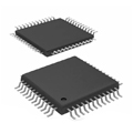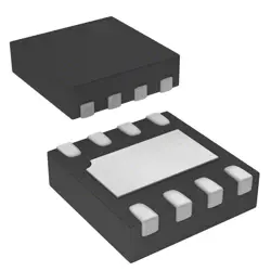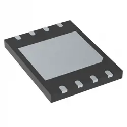

Bilder sind nur zur Referenz
SN74LVC2G126DCTR
IC BUFFER NON-INVERT 5.5V SM8
- Hersteller
- Fr. Teil #SN74LVC2G126DCTR
- Paket 8-LSSOP, 8-MSOP (0.110, 2.80mm Width)
- Datenblatt
- Auf Lager3882
100% Original und Neu
24 Stunden bereit zum Versand
365 Tage Garantie
RFQ & Erhalten Sie mehr Rabatte
Spezifikationen
| Package | Tape & Reel (TR),Cut Tape (CT) |
| Series | 74LVC |
| ProductStatus | Active |
| LogicType | Buffer, Non-Inverting |
| NumberofElements | 2 |
| NumberofBitsperElement | 1 |
| OutputType | 3-State |
| Current-OutputHighLow | 32mA, 32mA |
| Voltage-Supply | 1.65V ~ 5.5V |
| OperatingTemperature | -40°C ~ 125°C (TA) |
| MountingType | Surface Mount |
| Package/Case | 8-LSSOP, 8-MSOP (0.110, 2.80mm Width) |
Übersicht
Description
It has two independent buffer circuits that can drive capacitive loads, ideal for interfacing between different voltage levels or for signal conditioning applications. Each output can be enabled or disabled via a separate control input, allowing for flexible design configurations. The SN74LVC2G126DCTR comes in a small SOT-23 package, making it suitable for compact designs.
In summary, the SN74LVC2G126DCTR is a versatile and efficient component for voltage level shifting and buffering in various electronic circuits.
Features
1. Dual Buffers: Contains two independent buffers/drivers, enhancing flexibility in circuit design.
2. 3-State Outputs: Outputs can be set to high, low, or high impedance, allowing for easy bus sharing.
3. Voltage Range: Operates with a supply voltage range of 1.65V to 5.5V, making it compatible with various low-voltage systems.
4. High Speed: Offers fast propagation delays (typically 3.5 ns at 5V), suitable for high-speed applications.
5. Low Power Consumption: Consumes minimal power, ideal for battery-operated devices.
6. TTL Compatibility: Compatible with TTL logic levels for seamless integration into existing designs.
7. Package: Available in a small DFN package (SOT-23), optimizing space on PCBs.
Overall, the SN74LVC2G126DCTR is well-suited for applications requiring reliable signal buffering with minimal power usage.
Package
Pinout
Pin Functions:
1. A1 - Input for the first buffer.
2. Y1 - Output for the first buffer.
3. OE1 - Output Enable for the first buffer (active low).
4. A2 - Input for the second buffer.
5. Y2 - Output for the second buffer.
6. OE2 - Output Enable for the second buffer (active low).
7. GND - Ground connection.
8. VCC - Power supply connection.
The device is designed for low-voltage applications and features high-speed operation while providing low power consumption.
Manufacturer
Application
Equivalent
Versand
VersandmethodenWir
bieten Sie globale Versanddienstleistungen durch DHL, FedEx, TNT, UPS oder einen anderen Spediteur Ihrer Wahl.
Versandgebührenreferenz (DHL/FedEx):
DHL: Versandkosten reichen von $25-$45 (0.5kg), mit einer geschätzten Lieferzeit von 2-5 Werktagen.
von FedEx: Versandkosten reichen von $25-$40 (0.5kg), mit einer geschätzten Lieferzeit von 3-7 Werktagen.
UPS: Versandkosten reichen von $25-$45 (0.5kg), mit einer geschätzten Lieferzeit von 3-7 Werktagen.
TNT: Versandkosten reichen von $25-$65 (0.5kg), mit einer geschätzten Lieferzeit von 3-7 Werktagen.
EMS: Versandkosten reichen von $30-$50 (0.5kg), mit einer geschätzten Lieferzeit von 7-15 Werktagen.
Registrierte Luftpost: Versandkosten sind $ 2- $ 4 (0,1 kg), mit einer geschätzten Lieferzeit von 5-20 Werktagen.
Zahlungen
Payment Methods
Die Zahlungsfrist ist 100% Prepaid.
Derzeit akzeptieren wir nur die folgenden Zahlungsmethoden:
1. PayPal
2. Kredit- / Debitkarte
3. Überweisung
Ähnliche
-
![MX25R8035FM1IL0]() MX25R8035FM1IL0
Macronix
-
![MX25L3233FM1I-08Q]() MX25L3233FM1I-08Q
Macronix
-
![MX29F400CBTI-70G]() MX29F400CBTI-70G
Macronix
-
![MX25V16066M1I02]() MX25V16066M1I02
Macronix
-
![MX25V16066M2I02]() MX25V16066M2I02
Macronix
-
![MX29GL512FHXFI-11G]() MX29GL512FHXFI-11..
Macronix
-
![MX25U25643GZNI00]() MX25U25643GZNI00
Macronix
-
![MX25L2006EM1I-12G]() MX25L2006EM1I-12G
Macronix
-
![MX25R1635FZUIH0]() MX25R1635FZUIH0
Macronix
-
![MX25U6435FM2I-10G]() MX25U6435FM2I-10G
Macronix
-
![MX25U25645GXDI00]() MX25U25645GXDI00
Macronix
-
![MX25L12835FZ2I-10G]() MX25L12835FZ2I-10..
Macronix