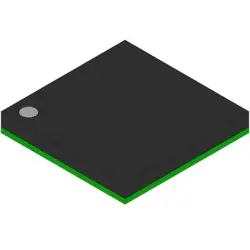
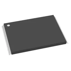
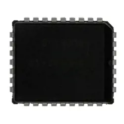
Bilder sind nur zur Referenz
TC7W74FU
Flip Flops
- Hersteller
- Fr. Teil #TC7W74FU
- Paket
- Datenblatt
- Auf Lager27148
100% Original und Neu
24 Stunden bereit zum Versand
365 Tage Garantie
RFQ & Erhalten Sie mehr Rabatte
Spezifikationen
Übersicht
Description
Key features of the TC7W74FU include:
- Dual Flip-Flops: Contains two independent D flip-flops.
- Edge Triggering: Operates on the rising or falling edge of a clock signal.
- Wide Supply Voltage Range: Typically operates at 2.0V to 5.5V, allowing flexibility in different circuit designs.
- Low Power Consumption: Efficient for battery-operated devices.
- TTL Compatibility: Can interface with standard TTL logic levels.
The TC7W74FU is commonly used in memory storage, data processing, and state machine applications, making it a versatile component in digital electronics.
Features
1. Dual D Flip-Flops: Contains two independent D flip-flops that can store one bit each.
2. Single Clock Input: Both flip-flops are clocked by a single clock input, allowing synchronous operation.
3. Asynchronous Set/Reset: Each flip-flop includes asynchronous set (S) and reset (R) inputs, enabling immediate state changes regardless of the clock.
4. Low Power Consumption: Designed for low power operation, making it suitable for battery-powered applications.
5. Wide Operating Voltage Range: Typically operates between 2V to 6V, providing flexibility in various circuits.
6. High-Speed Operation: Capable of high-speed switching, essential for modern digital circuits.
7. TTL Compatible: Compatible with Transistor-Transistor Logic (TTL) levels, facilitating integration with other digital logic families.
This IC is commonly used in counters, registers, and memory applications due to its reliable performance and simple interface.
Package
Pinout
Pin Configuration:
1. VCC (Pin 1): Power supply.
2. GND (Pin 8): Ground.
3. D1 (Pin 2): Data input for the first flip-flop.
4. D2 (Pin 3): Data input for the second flip-flop.
5. CLK1 (Pin 4): Clock input for the first flip-flop.
6. CLK2 (Pin 5): Clock input for the second flip-flop.
7. CLR1 (Pin 6): Clear input for the first flip-flop.
8. CLR2 (Pin 7): Clear input for the second flip-flop.
9. Q1 (Pin 9): Output for the first flip-flop.
10. Q2 (Pin 10): Output for the second flip-flop.
11. /Q1 (Pin 11): Inverted output for the first flip-flop.
12. /Q2 (Pin 12): Inverted output for the second flip-flop.
13. SET1 (Pin 13): Set input for the first flip-flop.
14. SET2 (Pin 14): Set input for the second flip-flop.
The TC7W74FU operates in CMOS technology, ensuring low power consumption and high-speed performance.
Manufacturer
Application
Equivalent
Versand
VersandmethodenWir
bieten Sie globale Versanddienstleistungen durch DHL, FedEx, TNT, UPS oder einen anderen Spediteur Ihrer Wahl.
Versandgebührenreferenz (DHL/FedEx):
DHL: Versandkosten reichen von $25-$45 (0.5kg), mit einer geschätzten Lieferzeit von 2-5 Werktagen.
von FedEx: Versandkosten reichen von $25-$40 (0.5kg), mit einer geschätzten Lieferzeit von 3-7 Werktagen.
UPS: Versandkosten reichen von $25-$45 (0.5kg), mit einer geschätzten Lieferzeit von 3-7 Werktagen.
TNT: Versandkosten reichen von $25-$65 (0.5kg), mit einer geschätzten Lieferzeit von 3-7 Werktagen.
EMS: Versandkosten reichen von $30-$50 (0.5kg), mit einer geschätzten Lieferzeit von 7-15 Werktagen.
Registrierte Luftpost: Versandkosten sind $ 2- $ 4 (0,1 kg), mit einer geschätzten Lieferzeit von 5-20 Werktagen.
Zahlungen
Payment Methods
Die Zahlungsfrist ist 100% Prepaid.
Derzeit akzeptieren wir nur die folgenden Zahlungsmethoden:
1. PayPal
2. Kredit- / Debitkarte
3. Überweisung
Ähnliche
-
![MX25L3233FM1I-08Q]() MX25L3233FM1I-08Q
Macronix
-
![MX25V1635FZNI]() MX25V1635FZNI
Macronix
-
![MX25V1635FZNQ03]() MX25V1635FZNQ03
Macronix
-
![MX30LF2G28AD-TI]() MX30LF2G28AD-TI
Macronix
-
![MX25L25673GMI-08G]() MX25L25673GMI-08G
Macronix
-
![MX29GL512FHXFI-11G]() MX29GL512FHXFI-11..
Macronix
-
![MX25V1635FM2I]() MX25V1635FM2I
Macronix
-
![MX25U6435FM2I-10G]() MX25U6435FM2I-10G
Macronix
-
![MX29LV160DTTI-70G]() MX29LV160DTTI-70G
Macronix
-
![MX29F040CQI-70G]() MX29F040CQI-70G
Macronix
-
![MX25L25645GXDI-08G]() MX25L25645GXDI-08..
Macronix
-
![MX29LV640ETTI-70G]() MX29LV640ETTI-70G
Macronix