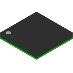
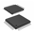
Bilder sind nur zur Referenz
TC7WH125FU
- Hersteller
- Fr. Teil #TC7WH125FU
- Paket
- Datenblatt
- Auf Lager8963
100% Original und Neu
24 Stunden bereit zum Versand
365 Tage Garantie
RFQ & Erhalten Sie mehr Rabatte
Spezifikationen
| Brand | Toshiba |
| Subcategory | Logic ICs |
| Product Type | Buffers & Line Drivers |
| Series | TC7WH125 |
| Logic Family | WH |
Übersicht
Description
Key features of the TC7WH125FU include its ability to provide two independent buffers with three-state outputs, which can drive up to 15 LSTTL (Low-power Schottky TTL) loads. This attribute is essential for applications requiring data line isolation and multiplexing. The device also includes over-voltage tolerant inputs, allowing for interface compatibility with 5V logic when operating at lower voltages.
Packaged in a small, surface-mount TSSOP (Thin Shrink Small Outline Package), the TC7WH125FU is suitable for compact circuit designs. Its low power dissipation and high-speed operation make it ideal for use in personal electronics, computing, and communication devices where efficient signal management is crucial.
Features
1. Logic Type: Dual buffer.
2. Input Type: CMOS, which offers high noise immunity and low static power consumption.
3. Output Type: Push-pull.
4. Voltage Range: Operates over a range of voltages, typically around 2V to 6V.
5. Temperature Range: Suitable for standard commercial operating temperatures.
6. Package: Available in small surface-mount packages like USV (SOT-353).
7. Propagation Delay: Fast switching speeds, contributing to efficient signal processing.
8. Power Consumption: Low power consumption due to CMOS technology, making it suitable for battery-powered applications.
This component is ideal for applications requiring signal buffering and enhancing driving capability without altering the signal integrity.
Package
Pinout
Regarding its pin count and function:
- Pin Count: The TC7WH125FU is housed in an 8-pin package.
- Function: It includes two independent buffer/drivers. Each buffer/driver has an input, an output, and an output enable pin. When the output enable pin is low, the corresponding output is disabled (high-impedance state), allowing for shared bus applications. When the output enable pin is high, the input signal is propagated to the output, providing a strong drive capability.
This functionality is useful for controlling data flow and isolating different parts of a circuit, ensuring that signals are transmitted accurately and efficiently while preventing possible contention on shared bus lines.
Manufacturer
Application
Equivalent
Versand
VersandmethodenWir
bieten Sie globale Versanddienstleistungen durch DHL, FedEx, TNT, UPS oder einen anderen Spediteur Ihrer Wahl.
Versandgebührenreferenz (DHL/FedEx):
DHL: Versandkosten reichen von $25-$45 (0.5kg), mit einer geschätzten Lieferzeit von 2-5 Werktagen.
von FedEx: Versandkosten reichen von $25-$40 (0.5kg), mit einer geschätzten Lieferzeit von 3-7 Werktagen.
UPS: Versandkosten reichen von $25-$45 (0.5kg), mit einer geschätzten Lieferzeit von 3-7 Werktagen.
TNT: Versandkosten reichen von $25-$65 (0.5kg), mit einer geschätzten Lieferzeit von 3-7 Werktagen.
EMS: Versandkosten reichen von $30-$50 (0.5kg), mit einer geschätzten Lieferzeit von 7-15 Werktagen.
Registrierte Luftpost: Versandkosten sind $ 2- $ 4 (0,1 kg), mit einer geschätzten Lieferzeit von 5-20 Werktagen.
Zahlungen
Payment Methods
Die Zahlungsfrist ist 100% Prepaid.
Derzeit akzeptieren wir nur die folgenden Zahlungsmethoden:
1. PayPal
2. Kredit- / Debitkarte
3. Überweisung
Ähnliche
-
![MX25L3233FM1I-08Q]() MX25L3233FM1I-08Q
Macronix
-
![MX25V1635FZNI]() MX25V1635FZNI
Macronix
-
![MX25R3235FZNIL0]() MX25R3235FZNIL0
Macronix
-
![MX25R6435FBDIL0]() MX25R6435FBDIL0
Macronix
-
![MX25L25673GMI-08G]() MX25L25673GMI-08G
Macronix
-
![MX25L25673GMI-10G]() MX25L25673GMI-10G
Macronix
-
![MX29GL512FHXFI-11G]() MX29GL512FHXFI-11..
Macronix
-
![MX25U51279GXDR00]() MX25U51279GXDR00
Macronix
-
![MX25U25643GZNI00]() MX25U25643GZNI00
Macronix
-
![MX25U6435FM2I-10G]() MX25U6435FM2I-10G
Macronix
-
![MX25L12833FM2I-10G]() MX25L12833FM2I-10..
Macronix
-
![MX25U25645GXDI00]() MX25U25645GXDI00
Macronix