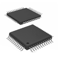

Bilder sind nur zur Referenz
TPS63020QDSJRQ1
IC REG BCK BST ADJ 3.5A 14VSON
- Hersteller
- Fr. Teil #TPS63020QDSJRQ1
- Paket VFDFN-14
- Datenblatt
- Auf Lager7691
100% Original und Neu
24 Stunden bereit zum Versand
365 Tage Garantie
RFQ & Erhalten Sie mehr Rabatte
Spezifikationen
| Package | Tape & Reel (TR),Cut Tape (CT) |
| Series | Automotive, AEC-Q100 |
| ProductStatus | Active |
| Function | Step-Up/Step-Down |
| OutputConfiguration | Positive |
| Topology | Buck-Boost |
| OutputType | Adjustable |
| NumberofOutputs | 1 |
| Voltage-Input(Min) | 1.8V |
| Voltage-Input(Max) | 5.5V |
| Voltage-Output(Min/Fixed) | 1.2V |
| Voltage-Output(Max) | 5.5V |
| Current-Output | 3.5A (Switch) |
| Frequency-Switching | 2.4MHz |
| SynchronousRectifier | Yes |
| OperatingTemperature | -40°C ~ 125°C (TJ) |
| MountingType | Surface Mount |
| Package/Case | 14-VFDFN Exposed Pad |
Übersicht
Description
Key features of the TPS63020QDSJRQ1 include:
- Wide input voltage range (1.8V to 5.5V), supporting single-cell lithium, two-cell alkaline, or NiMH batteries.
- Adjustable output voltage range from 1.2V to 5.5V.
- High efficiency up to 96% to maximize battery life.
- Output current capability up to 2A.
- Seamless transition between buck and boost modes.
- Low quiescent current of 50 μA, enhancing efficiency in low-power conditions.
- Integrated protection features, including overcurrent, thermal shutdown, and short-circuit protection.
- Automotive-grade qualification, ensuring reliability in automotive environments.
The compact design and robust performance make the TPS63020QDSJRQ1 ideal for portable electronics, automotive systems, and other applications requiring efficient power management.
Features
1. Wide Input Voltage Range: Operates from 1.8V to 5.5V, making it suitable for batteries or other variable sources.
2. Adjustable Output Voltage: Can be set between 1.2V to 5.5V using external resistors.
3. High Efficiency: Offers up to 96% efficiency, enhancing battery life in portable applications.
4. Seamless Transition: Effortlessly switches between buck and boost modes to maintain stable output.
5. Output Current Capability: Provides up to 2A output current in boost mode and 3A in buck mode.
6. Low Quiescent Current: Consumes minimal power during idle states, which is beneficial for battery-operated devices.
7. Protection Features: Includes overcurrent protection, short-circuit protection, and thermal shutdown for enhanced reliability.
8. Compact Size: Available in a 3mm x 3mm VSON package, suitable for space-constrained designs.
9. Automotive Qualification: AEC-Q100 qualified, ensuring it meets stringent automotive standards.
These features make it ideal for use in automotive, industrial, and consumer electronics requiring efficient power management.
Package
Pinout
Here's a brief overview of its pin functions:
1. VIN: Power input voltage.
2. GND: Ground connection.
3. VOUT: Regulated output voltage.
4. L1: Inductor connection for the buck-boost operation.
5. L2: Inductor connection for the buck-boost operation.
6. EN: Enable pin; activates the device when high.
7. PG: Power good indicator, open-drain output.
8. FB: Feedback pin for output voltage regulation.
9. PS/SYNC: Power Save Mode or external clock synchronization input.
10. MODE: Mode selection pin for automatic or forced PWM operation.
11. NC: No connection.
12. PGND: Power ground for switching circuitry.
13. AVIN: Analog input voltage for control circuitry.
14. SS: Soft start pin, controls the inrush current.
These pins allow for efficient energy conversion, supporting applications that require a stable output voltage across various input conditions.
Manufacturer
Application
Equivalent
1. LTC3115-1 from Analog Devices: A synchronous buck-boost converter.
2. MAX77813 from Maxim Integrated: A high-efficiency buck-boost converter.
3. ISL91110 from Renesas: A high-current buck-boost switching regulator.
4. NCP3135 from ON Semiconductor: A buck-boost DC-DC converter.
Each of these alternatives should be evaluated for specific application requirements such as input/output voltage range, current capability, efficiency, and package type.
Versand
VersandmethodenWir
bieten Sie globale Versanddienstleistungen durch DHL, FedEx, TNT, UPS oder einen anderen Spediteur Ihrer Wahl.
Versandgebührenreferenz (DHL/FedEx):
DHL: Versandkosten reichen von $25-$45 (0.5kg), mit einer geschätzten Lieferzeit von 2-5 Werktagen.
von FedEx: Versandkosten reichen von $25-$40 (0.5kg), mit einer geschätzten Lieferzeit von 3-7 Werktagen.
UPS: Versandkosten reichen von $25-$45 (0.5kg), mit einer geschätzten Lieferzeit von 3-7 Werktagen.
TNT: Versandkosten reichen von $25-$65 (0.5kg), mit einer geschätzten Lieferzeit von 3-7 Werktagen.
EMS: Versandkosten reichen von $30-$50 (0.5kg), mit einer geschätzten Lieferzeit von 7-15 Werktagen.
Registrierte Luftpost: Versandkosten sind $ 2- $ 4 (0,1 kg), mit einer geschätzten Lieferzeit von 5-20 Werktagen.
Zahlungen
Payment Methods
Die Zahlungsfrist ist 100% Prepaid.
Derzeit akzeptieren wir nur die folgenden Zahlungsmethoden:
1. PayPal
2. Kredit- / Debitkarte
3. Überweisung
Ähnliche
-
![MX25L3233FM1I-08Q]() MX25L3233FM1I-08Q
Macronix
-
![MX25V1635FZNI]() MX25V1635FZNI
Macronix
-
![MX66U1G45GXDI00]() MX66U1G45GXDI00
Macronix
-
![MX25V5126FM1I]() MX25V5126FM1I
Macronix
-
![MX25V4035FZUI]() MX25V4035FZUI
Macronix
-
![MX25V2033FM1I]() MX25V2033FM1I
Macronix
-
![MX30LF2G28AD-TI]() MX30LF2G28AD-TI
Macronix
-
![MX25L8035EM2I-10G]() MX25L8035EM2I-10G
Macronix
-
![MX25L25673GMI-08G]() MX25L25673GMI-08G
Macronix
-
![MX25L25673GMI-10G]() MX25L25673GMI-10G
Macronix
-
![MX25L2006EM1I-12G]() MX25L2006EM1I-12G
Macronix
-
![MX25V1635FM2I]() MX25V1635FM2I
Macronix