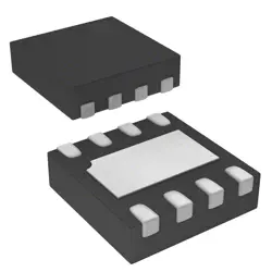
Bilder sind nur zur Referenz
XC6SLX75-2FGG484C
IC FPGA 280 I/O 484FBGA
- Hersteller
- Fr. Teil #XC6SLX75-2FGG484C
- Paket
- Datenblatt
- Auf Lager4724
100% Original und Neu
24 Stunden bereit zum Versand
365 Tage Garantie
RFQ & Erhalten Sie mehr Rabatte
Spezifikationen
| Series | Spartan®-6 LX |
| Part Status | Active |
| Base Product Number | XC6SLX75 |
| DigiKey Programmable | Not Verified |
| Number of LABs/CLBs | 5831 |
| Number of Logic Elements/Cells | 74637 |
| Total RAM Bits | 3170304 |
| Number of I/O | 280 |
| Voltage - Supply | 1.14V ~ 1.26V |
| Mounting Type | Surface Mount |
| Operating Temperature | 0°C ~ 85°C (TJ) |
| Package | 484-BBGA |
| Supplier Device Package | 484-FBGA (23x23) |
| Packaging | Tray |
Übersicht
Description
The "2" in the part number indicates the speed grade, which defines the performance characteristics, while "FGG" denotes the fine-pitch ball grid array (FBGA) package type, ensuring a compact footprint. The XC6SLX75-2FGG484C is well-suited for applications in communications, automotive, industrial control, and consumer electronics due to its balance of performance, power efficiency, and low cost. It is programmable using Xilinx's ISE Design Suite, enabling designers to leverage extensive development tools and IP cores for rapid prototyping and deployment.
Features
- Logic Cells: 75,000 system logic cells for complex designs.
- DSP Slices: Integrated DSP blocks for high-performance arithmetic operations.
- Block RAM: Up to 4.9 Mb of on-chip memory for data storage.
- I/O Pins: 484-ball package with flexible I/O configurations supporting various standards (e.g., LVDS, SSTL).
- Speed Grade: -2 indicates a maximum operating frequency of up to 200 MHz.
- Power Efficiency: Low power consumption, ideal for battery-operated or thermal-sensitive applications.
- Configurable Clock Management: Integrated clock management resources for efficient clock distribution.
- JTAG Support: Built-in support for JTAG programming and debugging.
This FPGA is suitable for applications in communications, automotive, industrial, and consumer electronics.
Package
Pinout
The functions of the pins include various I/O configurations supporting different standards such as LVTTL, LVCMOS, and HSTL. It features multiple power and ground connections, along with dedicated pins for configuration, clock inputs, and JTAG programming. The device supports differential signaling and has specific pins for dedicated clock management and high-speed transceivers, enhancing its versatility for a range of applications in digital design and embedded systems.
For detailed specifications, consulting the datasheet is recommended.
Manufacturer
Application
Equivalent
Versand
VersandmethodenWir
bieten Sie globale Versanddienstleistungen durch DHL, FedEx, TNT, UPS oder einen anderen Spediteur Ihrer Wahl.
Versandgebührenreferenz (DHL/FedEx):
DHL: Versandkosten reichen von $25-$45 (0.5kg), mit einer geschätzten Lieferzeit von 2-5 Werktagen.
von FedEx: Versandkosten reichen von $25-$40 (0.5kg), mit einer geschätzten Lieferzeit von 3-7 Werktagen.
UPS: Versandkosten reichen von $25-$45 (0.5kg), mit einer geschätzten Lieferzeit von 3-7 Werktagen.
TNT: Versandkosten reichen von $25-$65 (0.5kg), mit einer geschätzten Lieferzeit von 3-7 Werktagen.
EMS: Versandkosten reichen von $30-$50 (0.5kg), mit einer geschätzten Lieferzeit von 7-15 Werktagen.
Registrierte Luftpost: Versandkosten sind $ 2- $ 4 (0,1 kg), mit einer geschätzten Lieferzeit von 5-20 Werktagen.
Zahlungen
Payment Methods
Die Zahlungsfrist ist 100% Prepaid.
Derzeit akzeptieren wir nur die folgenden Zahlungsmethoden:
1. PayPal
2. Kredit- / Debitkarte
3. Überweisung
Ähnliche
-
![MX25R8035FM1IL0]() MX25R8035FM1IL0
MX25R8035FM1IL0
Macronix
-
![MX25L3233FZBI-08Q]() MX25L3233FZBI-08Q
MX25L3233FZBI-08Q
Macronix
-
![MX25V5126FM1I]() MX25V5126FM1I
MX25V5126FM1I
Macronix
-
![MX25V16066M1I02]() MX25V16066M1I02
MX25V16066M1I02
Macronix
-
![MX25R3235FZNIL0]() MX25R3235FZNIL0
MX25R3235FZNIL0
Macronix
-
![MX25R6435FBDIL0]() MX25R6435FBDIL0
MX25R6435FBDIL0
Macronix
-
![MX29GL512FHXFI-11G]() MX29GL512FHXFI-11..
MX29GL512FHXFI-11..
Macronix
-
![MX25R1635FZUIH0]() MX25R1635FZUIH0
MX25R1635FZUIH0
Macronix
-
![MX25V1635FM2I]() MX25V1635FM2I
MX25V1635FM2I
Macronix
-
![MX25U6435FM2I-10G]() MX25U6435FM2I-10G
MX25U6435FM2I-10G
Macronix
-
![MX25L12833FM2I-10G]() MX25L12833FM2I-10..
MX25L12833FM2I-10..
Macronix
-
![MX25L12833FZ2I-10G]() MX25L12833FZ2I-10..
MX25L12833FZ2I-10..
Macronix