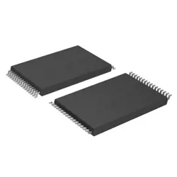
Bilder sind nur zur Referenz
XCKU040-2FFVA1156I
IC FPGA 520 I/O 1156FCBGA
- Hersteller
- Fr. Teil #XCKU040-2FFVA1156I
- Paket FCBGA-1156
- Datenblatt
- Auf Lager4883
100% Original und Neu
24 Stunden bereit zum Versand
365 Tage Garantie
RFQ & Erhalten Sie mehr Rabatte
Spezifikationen
| Package | Tray |
| Series | Kintex® UltraScale™ |
| ProductStatus | Active |
| NumberofLABs/CLBs | 30300 |
| NumberofLogicElements/Cells | 530250 |
| TotalRAMBits | 21606000 |
| NumberofI/O | 520 |
| Voltage-Supply | 0.922V ~ 0.979V |
| MountingType | Surface Mount |
| OperatingTemperature | -40°C ~ 100°C (TJ) |
| Package/Case | 1156-BBGA, FCBGA |
Übersicht
Description
The device incorporates advanced features such as high-speed serial transceivers, PCIe support, and the capability to implement complex algorithms in hardware. Its FFVA package type indicates a flip-chip design with a fine pitch, providing enhanced thermal performance and signal integrity. The "I" designation denotes industrial-grade reliability, suitable for harsh operating environments.
Overall, the XCKU040-2FFVA1156I is ideal for users seeking robust processing capabilities with the flexibility of FPGA architecture, enabling rapid prototyping and deployment of customizable hardware solutions.
Features
1. Logic Cells: Approximately 40K logic cells, enabling complex designs.
2. DSP Slices: 220 DSP48E1 slices for high-performance signal processing.
3. Memory: Up to 5.8 Mb of block RAM for data storage.
4. I/O: 540 user I/O pins with support for various I/O standards, including LVDS.
5. Transceivers: Up to 16 serial transceivers supporting speeds up to 12.5 Gbps.
6. Power Efficiency: Optimized for low power consumption with dynamic power management.
7. Configuration: Supports various configuration modes such as JTAG and SPI.
8. Architecture: Utilizes a 20nm process technology, enhancing performance and reducing size.
The XCKU040-2FFVA1156I is suitable for applications in communications, automotive, industrial, and more, providing a balance of performance and efficiency.
Package
Pinout
Manufacturer
Application
Equivalent
Versand
VersandmethodenWir
bieten Sie globale Versanddienstleistungen durch DHL, FedEx, TNT, UPS oder einen anderen Spediteur Ihrer Wahl.
Versandgebührenreferenz (DHL/FedEx):
DHL: Versandkosten reichen von $25-$45 (0.5kg), mit einer geschätzten Lieferzeit von 2-5 Werktagen.
von FedEx: Versandkosten reichen von $25-$40 (0.5kg), mit einer geschätzten Lieferzeit von 3-7 Werktagen.
UPS: Versandkosten reichen von $25-$45 (0.5kg), mit einer geschätzten Lieferzeit von 3-7 Werktagen.
TNT: Versandkosten reichen von $25-$65 (0.5kg), mit einer geschätzten Lieferzeit von 3-7 Werktagen.
EMS: Versandkosten reichen von $30-$50 (0.5kg), mit einer geschätzten Lieferzeit von 7-15 Werktagen.
Registrierte Luftpost: Versandkosten sind $ 2- $ 4 (0,1 kg), mit einer geschätzten Lieferzeit von 5-20 Werktagen.
Zahlungen
Payment Methods
Die Zahlungsfrist ist 100% Prepaid.
Derzeit akzeptieren wir nur die folgenden Zahlungsmethoden:
1. PayPal
2. Kredit- / Debitkarte
3. Überweisung
Ähnliche
-
![MX25V1635FZNQ03]() MX25V1635FZNQ03
MX25V1635FZNQ03
Macronix
-
![MX25V2033FM1I]() MX25V2033FM1I
MX25V2033FM1I
Macronix
-
![MX25V16066M1I02]() MX25V16066M1I02
MX25V16066M1I02
Macronix
-
![MX25V16066M2I02]() MX25V16066M2I02
MX25V16066M2I02
Macronix
-
![MX30LF2G28AD-TI]() MX30LF2G28AD-TI
MX30LF2G28AD-TI
Macronix
-
![MX25L8035EM2I-10G]() MX25L8035EM2I-10G
MX25L8035EM2I-10G
Macronix
-
![MX25R6435FBDIL0]() MX25R6435FBDIL0
MX25R6435FBDIL0
Macronix
-
![MX25L25673GMI-10G]() MX25L25673GMI-10G
MX25L25673GMI-10G
Macronix
-
![MX25U25643GZNI00]() MX25U25643GZNI00
MX25U25643GZNI00
Macronix
-
![MX25L25645GXDI-08G]() MX25L25645GXDI-08..
MX25L25645GXDI-08..
Macronix
-
![MX29F040CTI-70G]() MX29F040CTI-70G
MX29F040CTI-70G
Macronix
-
![MX25L4006EM2I-12G]() MX25L4006EM2I-12G
MX25L4006EM2I-12G
Macronix