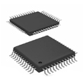

Bilder sind nur zur Referenz
XCKU15P-2FFVA1156I
IC FPGA 516 I/O 1156FCBGA
- Hersteller
- Fr. Teil #XCKU15P-2FFVA1156I
- Paket FCBGA-1156
- Datenblatt
- Auf Lager5636
100% Original und Neu
24 Stunden bereit zum Versand
365 Tage Garantie
RFQ & Erhalten Sie mehr Rabatte
Spezifikationen
| Package | Tray |
| Series | Kintex® UltraScale+™ |
| ProductStatus | Active |
| NumberofLABs/CLBs | 65340 |
| NumberofLogicElements/Cells | 1143450 |
| TotalRAMBits | 82329600 |
| NumberofI/O | 516 |
| Voltage-Supply | 0.825V ~ 0.876V |
| MountingType | Surface Mount |
| OperatingTemperature | -40°C ~ 100°C (TJ) |
| Package/Case | 1156-BBGA, FCBGA |
Übersicht
Description
Key specifications include a dual-mode (SRAM/Flash) configuration, support for high-speed serial transceivers, and an extensive array of I/O options. The device operates at high clock frequencies, enabling it to handle complex algorithms and real-time processing tasks efficiently.
The FFVA1156 package indicates a fine-pitch ball grid array (FBGA) with 1156 pins, allowing for dense integration and reduced board space. The "I" suffix denotes an industrial-grade variant, ensuring reliable operation across a wide temperature range.
Overall, the XCKU15P-2FFVA1156I is designed for scalability and flexibility, making it an ideal choice for developers looking to implement advanced digital designs in various demanding environments.
Features
1. Logic Cells: Approximately 15,000 logic cells for complex designs.
2. DSP Slices: Up to 60 DSP slices, suitable for high-speed digital signal processing tasks.
3. Memory: Supports embedded memory blocks, including up to 1.4 Mb of block RAM.
4. I/O Capabilities: Offers a wide range of I/O standards and up to 420 user I/O pins.
5. High-Speed Transceivers: Equipped with high-speed transceivers capable of 6.6 Gbps to support various communication protocols.
6. Power Efficiency: Designed for optimal power consumption, making it ideal for embedded and data center applications.
7. Configuration Options: Supports multiple configuration methods including JTAG and SPI.
This FPGA is suitable for applications in telecommunications, automotive, industrial automation, and video processing.
Package
Pinout
Functions of the pins include general-purpose I/O (GPIO), dedicated configuration, power supply, ground connections, and high-speed transceivers for data communication. The FPGA can be used in diverse applications such as communications, automotive, industrial, and data center solutions, providing flexibility for custom designs. The FPGA is housed in a flip-chip package, allowing for improved thermal performance and higher pin density.
Manufacturer
Application
Equivalent
Versand
VersandmethodenWir
bieten Sie globale Versanddienstleistungen durch DHL, FedEx, TNT, UPS oder einen anderen Spediteur Ihrer Wahl.
Versandgebührenreferenz (DHL/FedEx):
DHL: Versandkosten reichen von $25-$45 (0.5kg), mit einer geschätzten Lieferzeit von 2-5 Werktagen.
von FedEx: Versandkosten reichen von $25-$40 (0.5kg), mit einer geschätzten Lieferzeit von 3-7 Werktagen.
UPS: Versandkosten reichen von $25-$45 (0.5kg), mit einer geschätzten Lieferzeit von 3-7 Werktagen.
TNT: Versandkosten reichen von $25-$65 (0.5kg), mit einer geschätzten Lieferzeit von 3-7 Werktagen.
EMS: Versandkosten reichen von $30-$50 (0.5kg), mit einer geschätzten Lieferzeit von 7-15 Werktagen.
Registrierte Luftpost: Versandkosten sind $ 2- $ 4 (0,1 kg), mit einer geschätzten Lieferzeit von 5-20 Werktagen.
Zahlungen
Payment Methods
Die Zahlungsfrist ist 100% Prepaid.
Derzeit akzeptieren wir nur die folgenden Zahlungsmethoden:
1. PayPal
2. Kredit- / Debitkarte
3. Überweisung
Ähnliche
-
![MX29F400CBTI-70G]() MX29F400CBTI-70G
Macronix
-
![MX66U1G45GXDI00]() MX66U1G45GXDI00
Macronix
-
![MX25L25673GMI-08G]() MX25L25673GMI-08G
Macronix
-
![MX25R1635FZUIH0]() MX25R1635FZUIH0
Macronix
-
![MX25V1635FM2I]() MX25V1635FM2I
Macronix
-
![MX25U3232FZBI02]() MX25U3232FZBI02
Macronix
-
![MX25L12833FZ2I-10G]() MX25L12833FZ2I-10..
Macronix
-
![MX25L12833FZNI-10G]() MX25L12833FZNI-10..
Macronix
-
![MX29F040CQI-70G]() MX29F040CQI-70G
Macronix
-
![MX29LV640ETTI-70G]() MX29LV640ETTI-70G
Macronix
-
![MX25L1006EMI-10G]() MX25L1006EMI-10G
Macronix
-
![MX25V8035FM2I]() MX25V8035FM2I
Macronix