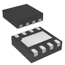
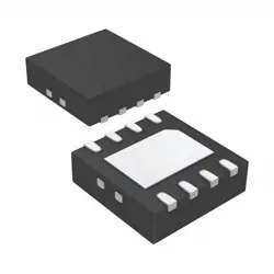
Bilder sind nur zur Referenz
ZL30143GGG2
IC SONET/SDH SYNCH 100CABGA
- Hersteller
- Fr. Teil #ZL30143GGG2
- Paket 100-FBGA
- Datenblatt
- Auf Lager2408
100% Original und Neu
24 Stunden bereit zum Versand
365 Tage Garantie
RFQ & Erhalten Sie mehr Rabatte
Spezifikationen
| Package | Tray |
| ProductStatus | Active |
| PLL | Yes |
| MainPurpose | Ethernet, SONET/SDH, Stratum |
| Input | Clock |
| Output | Clock |
| NumberofCircuits | 1 |
| Ratio-Input:Output | 13:14 |
| Differential-Input:Output | No/Yes |
| Frequency-Max | 622.08MHz |
| OperatingTemperature | -40°C ~ 85°C |
| MountingType | Surface Mount |
| Package/Case | 100-FBGA |
Übersicht
Description
Additionally, the ZL30143GGG2 is characterized by its ease of integration with existing systems, often requiring minimal external components. Its compact package size contributes to space-saving designs in electronic devices. The chip also includes built-in features for synchronization and error correction, enhancing reliability in critical timing applications. Overall, the ZL30143GGG2 is valued for its versatility, efficiency, and performance in delivering precise timing solutions.
Features
1. Multiple Output Frequencies: Supports a range of output frequencies, allowing flexibility in system design.
2. Low Jitter Performance: Provides high output precision with low jitter, crucial for high-speed data applications.
3. Integrated Phase-Locked Loop (PLL): Features an integrated PLL for frequency synthesis and stabilization.
4. Programmable Settings: Allows for programmable output settings via I2C or SPI interfaces, facilitating easy customization.
5. Power Management: Designed with low power consumption to enhance energy efficiency.
6. Wide Supply Voltage Range: Operates over a broad voltage range, making it suitable for various power supply configurations.
7. Compact Package: Available in a small form factor, enabling space-saving designs.
The ZL30143GGG2 is ideal for high-performance applications requiring accurate timing and signal integrity.
Package
Pinout
The main functions of the ZL30143 include clock recovery, synchronization, and jitter attenuation, making it suitable for various networking applications. It supports multiple input clock formats and provides flexible output options. Additionally, it offers features such as loop timing and frequency synthesis, which are essential for maintaining stable and accurate timing signals in high-speed data communication systems.
For precise pin assignments and detailed functionality, refer to the manufacturer's datasheet.
Manufacturer
Application
Equivalent
Versand
VersandmethodenWir
bieten Sie globale Versanddienstleistungen durch DHL, FedEx, TNT, UPS oder einen anderen Spediteur Ihrer Wahl.
Versandgebührenreferenz (DHL/FedEx):
DHL: Versandkosten reichen von $25-$45 (0.5kg), mit einer geschätzten Lieferzeit von 2-5 Werktagen.
von FedEx: Versandkosten reichen von $25-$40 (0.5kg), mit einer geschätzten Lieferzeit von 3-7 Werktagen.
UPS: Versandkosten reichen von $25-$45 (0.5kg), mit einer geschätzten Lieferzeit von 3-7 Werktagen.
TNT: Versandkosten reichen von $25-$65 (0.5kg), mit einer geschätzten Lieferzeit von 3-7 Werktagen.
EMS: Versandkosten reichen von $30-$50 (0.5kg), mit einer geschätzten Lieferzeit von 7-15 Werktagen.
Registrierte Luftpost: Versandkosten sind $ 2- $ 4 (0,1 kg), mit einer geschätzten Lieferzeit von 5-20 Werktagen.
Zahlungen
Payment Methods
Die Zahlungsfrist ist 100% Prepaid.
Derzeit akzeptieren wir nur die folgenden Zahlungsmethoden:
1. PayPal
2. Kredit- / Debitkarte
3. Überweisung
Ähnliche
-
![MX25L3233FZBI-08Q]() MX25L3233FZBI-08Q
MX25L3233FZBI-08Q
Macronix
-
![MX25L3233FM1I-08Q]() MX25L3233FM1I-08Q
MX25L3233FM1I-08Q
Macronix
-
![MX25V4035FZUI]() MX25V4035FZUI
MX25V4035FZUI
Macronix
-
![MX25V2033FM1I]() MX25V2033FM1I
MX25V2033FM1I
Macronix
-
![MX25V16066M2I02]() MX25V16066M2I02
MX25V16066M2I02
Macronix
-
![MX25L8035EM2I-10G]() MX25L8035EM2I-10G
MX25L8035EM2I-10G
Macronix
-
![MX25U25643GZNI00]() MX25U25643GZNI00
MX25U25643GZNI00
Macronix
-
![MX25U3232FZBI02]() MX25U3232FZBI02
MX25U3232FZBI02
Macronix
-
![MX25L12833FZ2I-10G]() MX25L12833FZ2I-10..
MX25L12833FZ2I-10..
Macronix
-
![MX25L12833FZNI-10G]() MX25L12833FZNI-10..
MX25L12833FZNI-10..
Macronix
-
![MX25L25645GXDI-08G]() MX25L25645GXDI-08..
MX25L25645GXDI-08..
Macronix
-
![MX29LV640ETTI-70G]() MX29LV640ETTI-70G
MX29LV640ETTI-70G
Macronix